Hode Computer - Talk
* arch decisions
* processor only, use RasPi for memory and IO
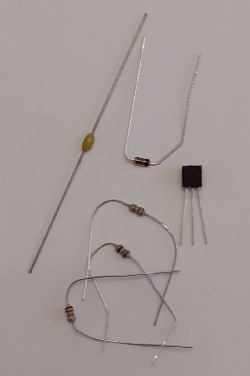
* use BJTs, diodes, resistors, capacitors
no flower (germanium) transistors, too expensive
just dirt/sand-cheap silicon
 * no MOSFETs or ICs
 * not a toy - useable address space, interrupts
* byte addressable memory, no 12-bit or 18-bit nonsense
* other than that, dead simple to minimize transistor count
* 6800-like 8-bit still requires 16-bit adder
* not a toy - useable address space, interrupts
* byte addressable memory, no 12-bit or 18-bit nonsense
* other than that, dead simple to minimize transistor count
* 6800-like 8-bit still requires 16-bit adder
 8 & 16-bit accumulators
two 16-bit index registers
16-bit program counter
complex instructions
4000+ transistors
* could do IBM-1130-like (accumulator) but add bytes
would need 16-bit accum register, PC register, couple index registers
* PDP-11 has 8 16-bit registers, one is PC
8 & 16-bit accumulators
two 16-bit index registers
16-bit program counter
complex instructions
4000+ transistors
* could do IBM-1130-like (accumulator) but add bytes
would need 16-bit accum register, PC register, couple index registers
* PDP-11 has 8 16-bit registers, one is PC
 addressing modes complex, would need lots of states
* do Alpha/ARM-like 16-bit RISC with PDP-11-style registers
load/store for memory access (byte and word sized)
arithmetic on registers only
branches need condition code register
having PC be a regular register means don't need separate instructions for return, table jumps, etc
dead simple to implement
* needed registers
8 16-bit registers R0..R7, R7 is PC
could get by with 4 or 6 registers
5-bit processor status PS (interrupt enable IE + condition codes NZVC)
+------+-------------------+-----+-----+-----+-----+
| IE | . . . | N | Z | V | C |
+------+-------------------+-----+-----+-----+-----+
16-bit instruction register IR
state flipflops (turns out need 24)
* interrupts
* since just one interrupt request line,
save PC,PS in fixed memory locations FFFC,FFFE
start of interrupt service routine is 0002
no need for hardware stack pointer
* need return from interrupt instruction to restore PC,PS
* instructions, fixed 16-bit width for simplicity
loads/stores
arithmetics
branches
miscellaneous
read/write PSW (cond codes, interrupt enable)
return from interrupt
halt (or wait for interrupt)
IR[15:13] = major opcode
IR[12:10] = A register
IR[09:07] = D register
IR[06:04] = B register
IR[03:00] = minor opcode
+---.---.---+---.---.---+---.---.---+---.---.---+---.---.---.---+
| major | A-reg | D-reg | B-reg | minor |
+---.---.---+---.---.---+---.---.---+---.---.---+---.---.---.---+
13 10 7 4 0
loads/stores use A for address register, D for data register
B and minorop fields used for 7-bit signed offset
+---.---.---+---.---.---+---.---.---+---.---.---.---.---.---.---+
| major | A-reg | D-reg | byte offset |
+---.---.---+---.---.---+---.---.---+---.---.---.---.---.---.---+
13 10 7 0
arithmetics use A,B registers for ALU inputs
ALU output written to D register
minorop says which op to perform (ADD, SUB, AND, etc)
+---.---.---+---.---.---+---.---.---+---.---.---+---.---.---.---+
| 0 0 1 | A-reg | D-reg | B-reg | minor |
+---.---.---+---.---.---+---.---.---+---.---.---+---.---.---.---+
13 10 7 4 0
branches:
[12:10,00] = branch condition (non-zero)
[09:01] = signed word displacement
+---.---.---+---.---.---+---.---.---.---.---.---.---.---.---+---+
| 0 0 0 | cond | word offset | c |
+---.---.---+---.---.---+---.---.---.---.---.---.---.---.---+---+
13 10 1 0
miscellaneous:
[15:10,00] = zeroes
[02:01] = minorop says which misc instr
00 HALT sends B-reg to RasPi for halt reason
01 IRET doesn't use any other fields
10 WRPS uses B-reg to select register
11 RDPS uses D-reg to select register
+---.---.---.---.---.---+---.---.---+---.---.---+---.---.---.---+
| 0 0 0 0 0 0 | D-reg | B-reg | x | minor | 0 |
+---.---.---.---.---.---+---.---.---+---.---.---+---.---.---.---+
10 7 4 3 1 0
* transistor estimates
* registers: 6 x 16 x 8 = 800 + 20% for control = 1000
actual: 1200 (newer design 1080)
* alu: 20 x 16 = 320 (3 xors, and, or, multiplexor, decoding)
actual: 440 (newer design 380)
* ir: 5 x 16 = 80; psw: 6 x 5 = 30; raspi intf: 3 x 16 + 10 = 60
80 + 30 + 60 = 170 + 20% connection = 200
actual: 270
* seq: 24 x 6 = 144 + 100% decoders = 300
actual: 200
* total: 1000 + 300 + 200 + 300 = 1800
actual: 1200 + 440 + 270 + 200 = 2110
1 sq in per gate = 1800 sq in required
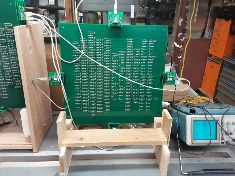
largest board can be made is 500mm x 500mm or 19.5in x 19.5in
18 x 18 with margins = 300 transistors per board = 6 boards
actually need 8 boards
* data & ctrl block diagrams
+-------------+
+------< <B |
| | REGISTERS D< <--+ . . . 4 x regboard
| +--< <A | |
| | a +-------------+ |
| | b |
| | u |
| | s |
| | +-------------+ |
| +--> >A | | d
b | | ALU D> >--+ b . . 2 x aluboard
b +------> >B | | u
u | +-------------+ | s
s | |
| . . . . . . . . . . . | &
| . . |
| . +-------------+ . | c
| . | | . | a
+------< <B PSW D< <--+ r
| . | | . | r
| . +-------------+ . | i
| . . | e
| . . | s
| . . |
| . +-------------+ . |
| . | | . |
+------< <B BCONS | . |
| . | | . |
| . +-------------+ . |
| . . |
| . . |
| . . |
| . +-------------+ . |
+------< <B | . |
. | RASPI MD< <--+
+--< <MQ | .
| . +-------------+ . . . . . rasboard
| . .
| . .
| . .
| . +-------------+ . +-------------+ . . . seqboard
| . | | . | |
+--> >D INSTREG Q> >------> >I SEQUENCER C> >------>
. | | ibus | | cbus
. +-------------+ . +-------------+
. . . . . . . . . . .
* busses & board contents
* abus & bbus, controls, ibus, dbus & carries
addressing modes complex, would need lots of states
* do Alpha/ARM-like 16-bit RISC with PDP-11-style registers
load/store for memory access (byte and word sized)
arithmetic on registers only
branches need condition code register
having PC be a regular register means don't need separate instructions for return, table jumps, etc
dead simple to implement
* needed registers
8 16-bit registers R0..R7, R7 is PC
could get by with 4 or 6 registers
5-bit processor status PS (interrupt enable IE + condition codes NZVC)
+------+-------------------+-----+-----+-----+-----+
| IE | . . . | N | Z | V | C |
+------+-------------------+-----+-----+-----+-----+
16-bit instruction register IR
state flipflops (turns out need 24)
* interrupts
* since just one interrupt request line,
save PC,PS in fixed memory locations FFFC,FFFE
start of interrupt service routine is 0002
no need for hardware stack pointer
* need return from interrupt instruction to restore PC,PS
* instructions, fixed 16-bit width for simplicity
loads/stores
arithmetics
branches
miscellaneous
read/write PSW (cond codes, interrupt enable)
return from interrupt
halt (or wait for interrupt)
IR[15:13] = major opcode
IR[12:10] = A register
IR[09:07] = D register
IR[06:04] = B register
IR[03:00] = minor opcode
+---.---.---+---.---.---+---.---.---+---.---.---+---.---.---.---+
| major | A-reg | D-reg | B-reg | minor |
+---.---.---+---.---.---+---.---.---+---.---.---+---.---.---.---+
13 10 7 4 0
loads/stores use A for address register, D for data register
B and minorop fields used for 7-bit signed offset
+---.---.---+---.---.---+---.---.---+---.---.---.---.---.---.---+
| major | A-reg | D-reg | byte offset |
+---.---.---+---.---.---+---.---.---+---.---.---.---.---.---.---+
13 10 7 0
arithmetics use A,B registers for ALU inputs
ALU output written to D register
minorop says which op to perform (ADD, SUB, AND, etc)
+---.---.---+---.---.---+---.---.---+---.---.---+---.---.---.---+
| 0 0 1 | A-reg | D-reg | B-reg | minor |
+---.---.---+---.---.---+---.---.---+---.---.---+---.---.---.---+
13 10 7 4 0
branches:
[12:10,00] = branch condition (non-zero)
[09:01] = signed word displacement
+---.---.---+---.---.---+---.---.---.---.---.---.---.---.---+---+
| 0 0 0 | cond | word offset | c |
+---.---.---+---.---.---+---.---.---.---.---.---.---.---.---+---+
13 10 1 0
miscellaneous:
[15:10,00] = zeroes
[02:01] = minorop says which misc instr
00 HALT sends B-reg to RasPi for halt reason
01 IRET doesn't use any other fields
10 WRPS uses B-reg to select register
11 RDPS uses D-reg to select register
+---.---.---.---.---.---+---.---.---+---.---.---+---.---.---.---+
| 0 0 0 0 0 0 | D-reg | B-reg | x | minor | 0 |
+---.---.---.---.---.---+---.---.---+---.---.---+---.---.---.---+
10 7 4 3 1 0
* transistor estimates
* registers: 6 x 16 x 8 = 800 + 20% for control = 1000
actual: 1200 (newer design 1080)
* alu: 20 x 16 = 320 (3 xors, and, or, multiplexor, decoding)
actual: 440 (newer design 380)
* ir: 5 x 16 = 80; psw: 6 x 5 = 30; raspi intf: 3 x 16 + 10 = 60
80 + 30 + 60 = 170 + 20% connection = 200
actual: 270
* seq: 24 x 6 = 144 + 100% decoders = 300
actual: 200
* total: 1000 + 300 + 200 + 300 = 1800
actual: 1200 + 440 + 270 + 200 = 2110
1 sq in per gate = 1800 sq in required
largest board can be made is 500mm x 500mm or 19.5in x 19.5in
18 x 18 with margins = 300 transistors per board = 6 boards
actually need 8 boards
* data & ctrl block diagrams
+-------------+
+------< <B |
| | REGISTERS D< <--+ . . . 4 x regboard
| +--< <A | |
| | a +-------------+ |
| | b |
| | u |
| | s |
| | +-------------+ |
| +--> >A | | d
b | | ALU D> >--+ b . . 2 x aluboard
b +------> >B | | u
u | +-------------+ | s
s | |
| . . . . . . . . . . . | &
| . . |
| . +-------------+ . | c
| . | | . | a
+------< <B PSW D< <--+ r
| . | | . | r
| . +-------------+ . | i
| . . | e
| . . | s
| . . |
| . +-------------+ . |
| . | | . |
+------< <B BCONS | . |
| . | | . |
| . +-------------+ . |
| . . |
| . . |
| . . |
| . +-------------+ . |
+------< <B | . |
. | RASPI MD< <--+
+--< <MQ | .
| . +-------------+ . . . . . rasboard
| . .
| . .
| . .
| . +-------------+ . +-------------+ . . . seqboard
| . | | . | |
+--> >D INSTREG Q> >------> >I SEQUENCER C> >------>
. | | ibus | | cbus
. +-------------+ . +-------------+
. . . . . . . . . . .
* busses & board contents
* abus & bbus, controls, ibus, dbus & carries
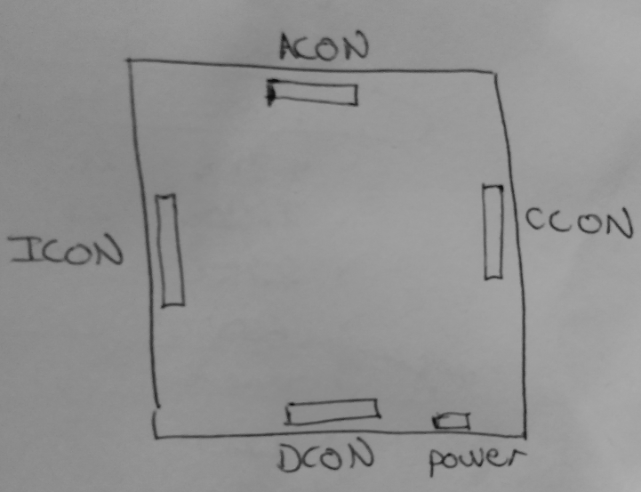 * primary input on left, primary output on right
* seq: input ibus, output controls
holds state flipflops, instruction decoding, control encoding
* ras: input dbus, output bbus
holds raspberry pi and interfacing, processor status word, instruction register
secondary output ibus
also drives clock, reset, intreq, intenab, branchtrue controls
rotated 90deg ccw
* alu: input abus & bbus, output dbus & carries
each board is an 8-bit alu
combinational logic only
jumpers determine which byte each board does
rotated 90deg cw
* reg: input dbus, output abus & ibus
each board holds 2 16-bit registers
jumpers determine which even/odd register pair the board is for
processor runs with minimum of one register board containing R6/R7
...but not terribly useful cuz arithmetic is register-to-register only
rotated 90deg ccw
* states
* primary input on left, primary output on right
* seq: input ibus, output controls
holds state flipflops, instruction decoding, control encoding
* ras: input dbus, output bbus
holds raspberry pi and interfacing, processor status word, instruction register
secondary output ibus
also drives clock, reset, intreq, intenab, branchtrue controls
rotated 90deg ccw
* alu: input abus & bbus, output dbus & carries
each board is an 8-bit alu
combinational logic only
jumpers determine which byte each board does
rotated 90deg cw
* reg: input dbus, output abus & ibus
each board holds 2 16-bit registers
jumpers determine which even/odd register pair the board is for
processor runs with minimum of one register board containing R6/R7
...but not terribly useful cuz arithmetic is register-to-register only
rotated 90deg ccw
* states
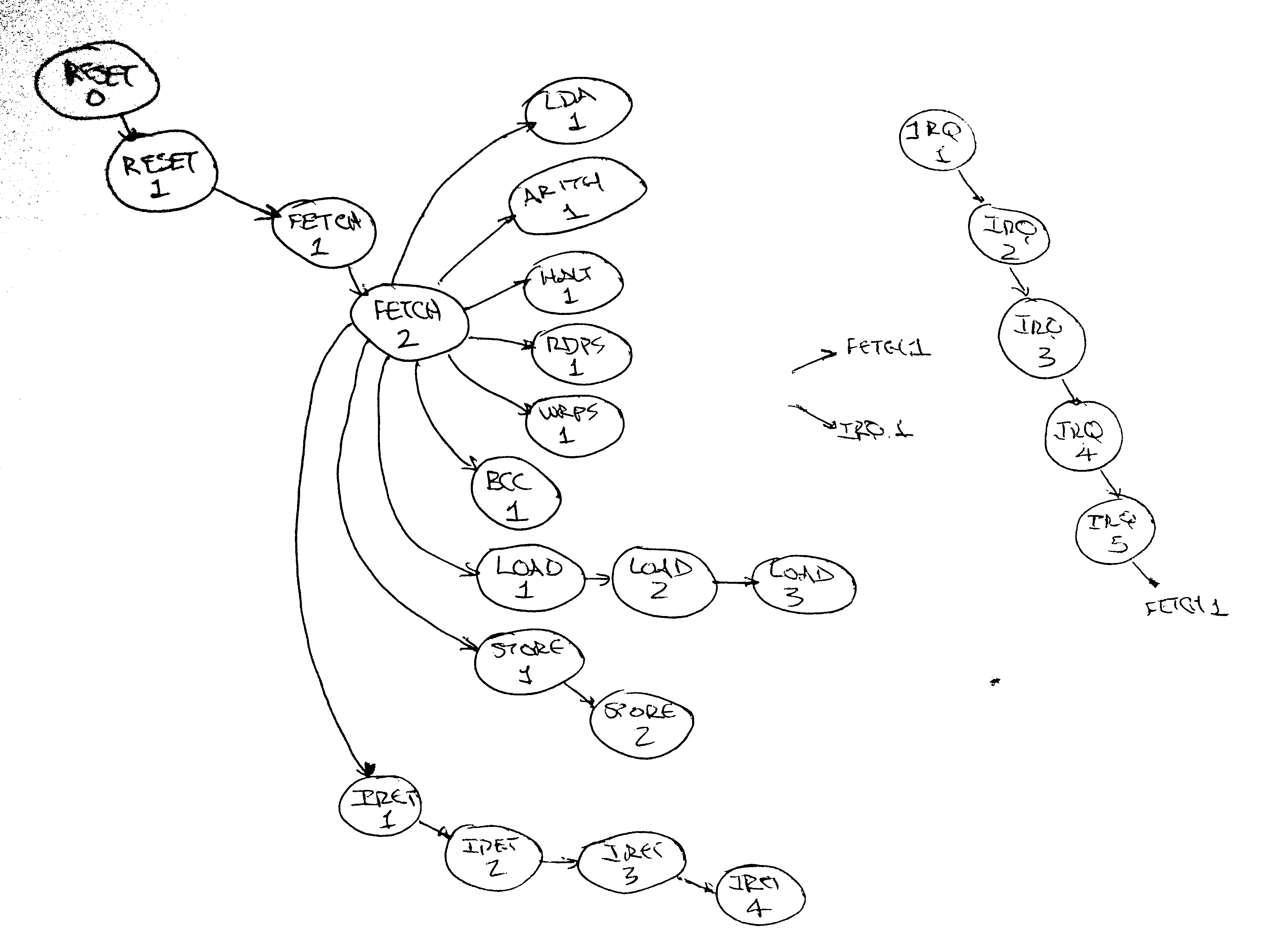 RESET.0 waits here as long as async RESET signal is asserted from RasPi
RESET.1 clocks here after RESET negated on next positive clock edge from RasPI
FETCH.1 sends PC to RasPi and asserts MEM_READ to start reading instruction
FETCH.2 receives instruction from RasPi and increments PC via the ALU
BCC.1 computes new PC via the ALU and decides whether or not to write PC by end of cycle
ARITH.1 does arithmetic on two registers via ALU and writes result to third at end of cycle and updates condition codes
LDA.1 adds offset to address register and writes result to data register at end of cycle
LOAD.1 adds offset to address register and sends to RasPi along with MEM_READ to start a read cycle
LOAD.2 receives data from RasPi and writes to data register at end of cycle
LOAD.3 if LD Rx,0(PC) this state increments PC over the immediate operand
STORE.1 adds offset to address register and sends to RasPi along with MEM_WRITE to start a write cycle
STORE.2 send data register to RasPi giving the data to be written
RDPS.1 gates PS through ALU and writes D register at end of cycle
WRPS.1 gates B register through ALU and writes to PS at end of cycle
HALT.1 gates B register through ALU on to RasPi and asserts HALT signal to RasPi
RasPi can stop clocking processor, processor continues with program when RasPi resumes clocking
IRET.1 send FFFC to RasPi along with MEM_READ to start reading saved PC from memory
IRET.2 receive saved PC value from RasPi and write to R7 (PC) at end of cycle
IRET.3 send FFFE to RasPi along with MEM_READ to start reading saved PS from memory
IRET.4 receive saved PS value from RasPi and write to PS at end of cycle
IREQ.1 send FFFE to RasPi along with MEM_WRITE to start writing saved PS to memory
IREQ.2 gate PS through ALU to RasPi to write to memory location FFFE
IREQ.3 send FFFC to RasPi along with MEM_WRITE to start writing saved PC to memory
IREQ.4 gate PC through ALU to RasPi to write to memory location FFFC ; clear PS<IE> bit
IREQ.5 send 0002 through ALU to write to R7 (PC) at end of cycle
* clocking
driven by RasPi GPIO pin CLK2 -> _CLK1 -> CLK0
mostly D flipflops clocked on leading edge of clock
IR latch open during FETCH2
RasPi takes sample just before raising clock
persists read data until halfway through next cycle
* raspi interface
Raspberry PI provides memory and IO via the GPIO connector.
+-------------------+ +--------+
| | | |
| Raspberry PI G | ---> clock,reset,intreq ---> | Hode |
| P | | CPU |
| I | <--- halt,memread,write,word <--- | |
| O | | |
| | <---- address[16]/data[16] ----> | |
| | | |
+-------------------+ +--------+
Signals from raspi to processor:
clock
reset
intreq
Signals from processor to raspi:
memory read
memory write
word vs byte
halted
+ 16-bit bi-directional address/data bus
* electrics
basic gate is and-or-invert
RESET.0 waits here as long as async RESET signal is asserted from RasPi
RESET.1 clocks here after RESET negated on next positive clock edge from RasPI
FETCH.1 sends PC to RasPi and asserts MEM_READ to start reading instruction
FETCH.2 receives instruction from RasPi and increments PC via the ALU
BCC.1 computes new PC via the ALU and decides whether or not to write PC by end of cycle
ARITH.1 does arithmetic on two registers via ALU and writes result to third at end of cycle and updates condition codes
LDA.1 adds offset to address register and writes result to data register at end of cycle
LOAD.1 adds offset to address register and sends to RasPi along with MEM_READ to start a read cycle
LOAD.2 receives data from RasPi and writes to data register at end of cycle
LOAD.3 if LD Rx,0(PC) this state increments PC over the immediate operand
STORE.1 adds offset to address register and sends to RasPi along with MEM_WRITE to start a write cycle
STORE.2 send data register to RasPi giving the data to be written
RDPS.1 gates PS through ALU and writes D register at end of cycle
WRPS.1 gates B register through ALU and writes to PS at end of cycle
HALT.1 gates B register through ALU on to RasPi and asserts HALT signal to RasPi
RasPi can stop clocking processor, processor continues with program when RasPi resumes clocking
IRET.1 send FFFC to RasPi along with MEM_READ to start reading saved PC from memory
IRET.2 receive saved PC value from RasPi and write to R7 (PC) at end of cycle
IRET.3 send FFFE to RasPi along with MEM_READ to start reading saved PS from memory
IRET.4 receive saved PS value from RasPi and write to PS at end of cycle
IREQ.1 send FFFE to RasPi along with MEM_WRITE to start writing saved PS to memory
IREQ.2 gate PS through ALU to RasPi to write to memory location FFFE
IREQ.3 send FFFC to RasPi along with MEM_WRITE to start writing saved PC to memory
IREQ.4 gate PC through ALU to RasPi to write to memory location FFFC ; clear PS<IE> bit
IREQ.5 send 0002 through ALU to write to R7 (PC) at end of cycle
* clocking
driven by RasPi GPIO pin CLK2 -> _CLK1 -> CLK0
mostly D flipflops clocked on leading edge of clock
IR latch open during FETCH2
RasPi takes sample just before raising clock
persists read data until halfway through next cycle
* raspi interface
Raspberry PI provides memory and IO via the GPIO connector.
+-------------------+ +--------+
| | | |
| Raspberry PI G | ---> clock,reset,intreq ---> | Hode |
| P | | CPU |
| I | <--- halt,memread,write,word <--- | |
| O | | |
| | <---- address[16]/data[16] ----> | |
| | | |
+-------------------+ +--------+
Signals from raspi to processor:
clock
reset
intreq
Signals from processor to raspi:
memory read
memory write
word vs byte
halted
+ 16-bit bi-directional address/data bus
* electrics
basic gate is and-or-invert
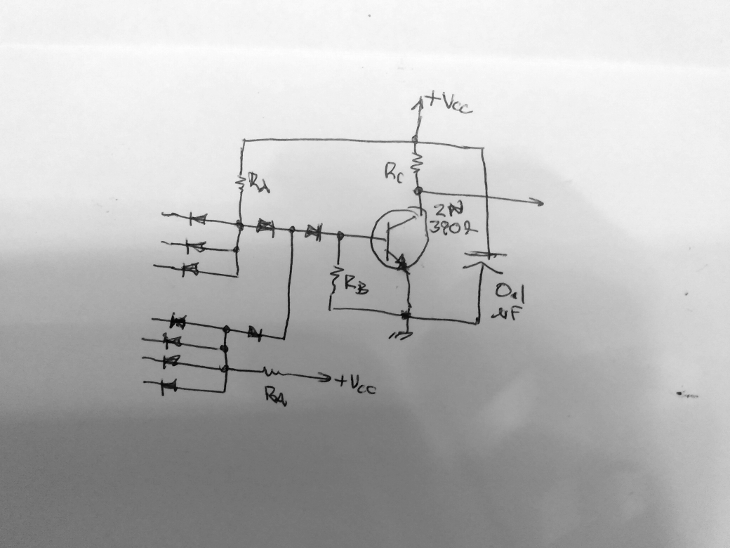
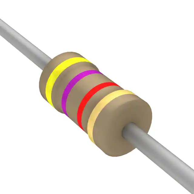
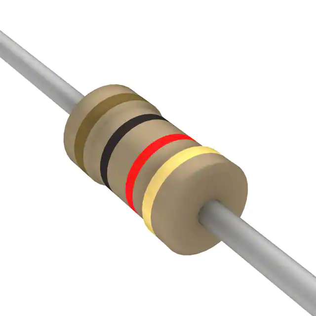
 2N3904 5 cents ea
capacitors 5 cents ea
diodes/resistors 1 cent ea
2N3904 peak beta 100 at ic=10mA, tapers to 80 at 25mA
operate at 10-25mA for fanout 1-10
Rc = 680
Ra = 2.7K
Rb base resistor
2N3904 5 cents ea
capacitors 5 cents ea
diodes/resistors 1 cent ea
2N3904 peak beta 100 at ic=10mA, tapers to 80 at 25mA
operate at 10-25mA for fanout 1-10
Rc = 680
Ra = 2.7K
Rb base resistor
 4.7K ~300nS low-to-high, mininum beta 25 needed for fanout 10
 1.0K <100nS low-to-high, minimum beta 60 needed for fanout 10
Originally built using 4.7K resistors for Rb. Processor ran at just under 70KHz (14.3uS).
Rebuilt lower ALU board with 1.0K resistors and added carry look-ahead.
Runs an hair above 84KHz (11.9uS) now, a 20% improvement.
dffs are 6 2- or 3-input nand gates
1.0K <100nS low-to-high, minimum beta 60 needed for fanout 10
Originally built using 4.7K resistors for Rb. Processor ran at just under 70KHz (14.3uS).
Rebuilt lower ALU board with 1.0K resistors and added carry look-ahead.
Runs an hair above 84KHz (11.9uS) now, a 20% improvement.
dffs are 6 2- or 3-input nand gates
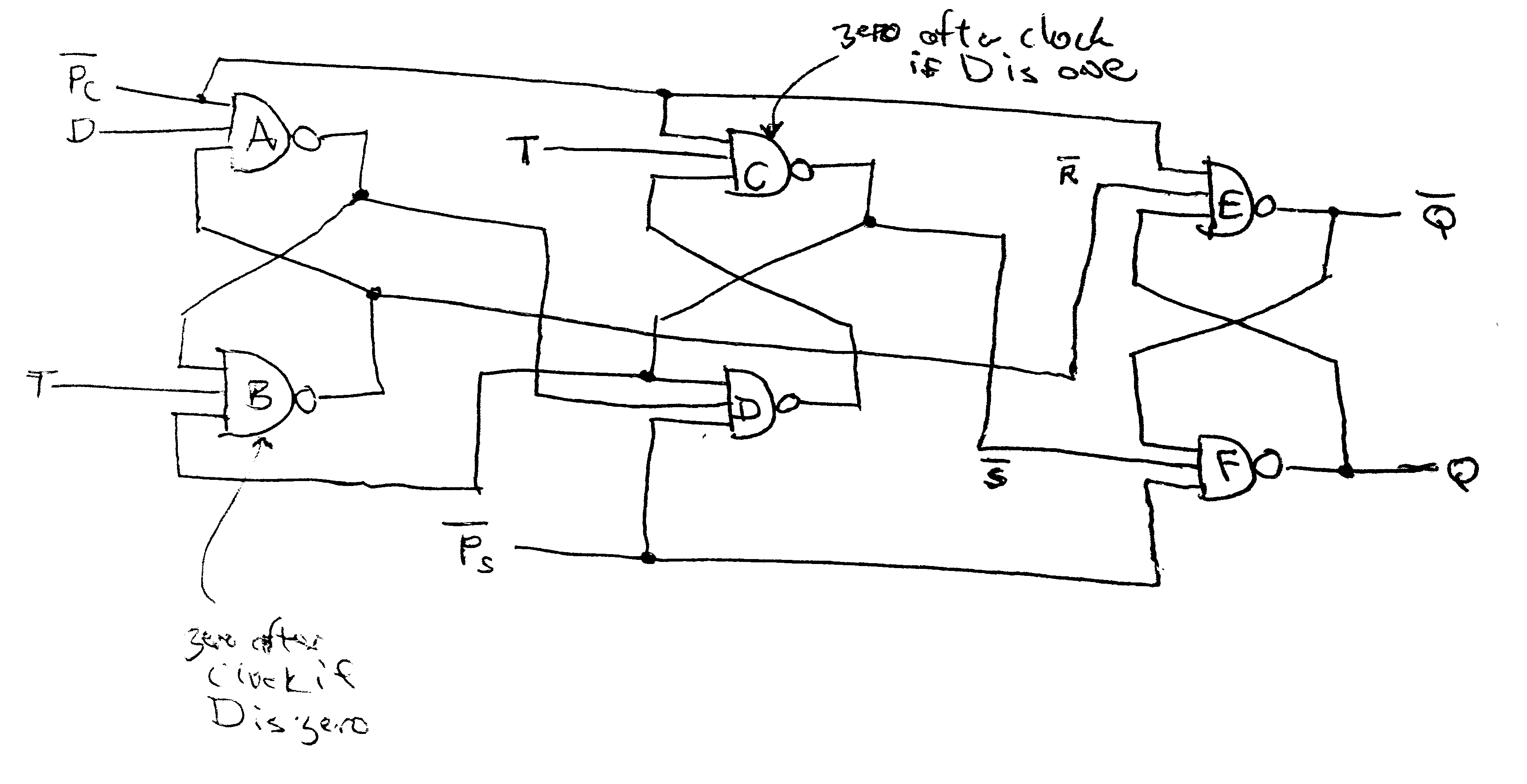
 latches are 4 2-input nand gates
similar raspi level converters
* netgen
design written in simplified Verilog-like language
module, wire, assign
assign supports & | ~
built-in modules for connector, D-flipflop, latch, raspberry-pi
netgen java program compiles then simulates and generates
simulation scripts written in tcl (like qvartvs), simulates at gate level
generation creates kicad net and pcb files (looks like scheme) and a report
needs a map file for placement at gate and flipflop level
gate and flipflop internals are pre-routed
* raspictl
generates clock, reset, intreq signals
receives memread, memwrite, halt signals
operates bi-directional data bus
shadows processor state for verification
contains 64K byte array for memory
check for magic memory location (FFF0) access by processor for IO
used for synchronous syscalls
processor program generates an argument block somewhere in memory
...then writes its address to FFF0
RasPi then parses the argument block and performs corresponding IO
when IO is complete, RasPi resumes clocking the processor
processor program reads IO status from FFF0
currently does exit(), close(), gettimeofday(), open(), read(), write()
...also can assert/negate interrupt request line for testing
and simple println() call for debugging
can also generate random opcodes and operands for testing
* test programs
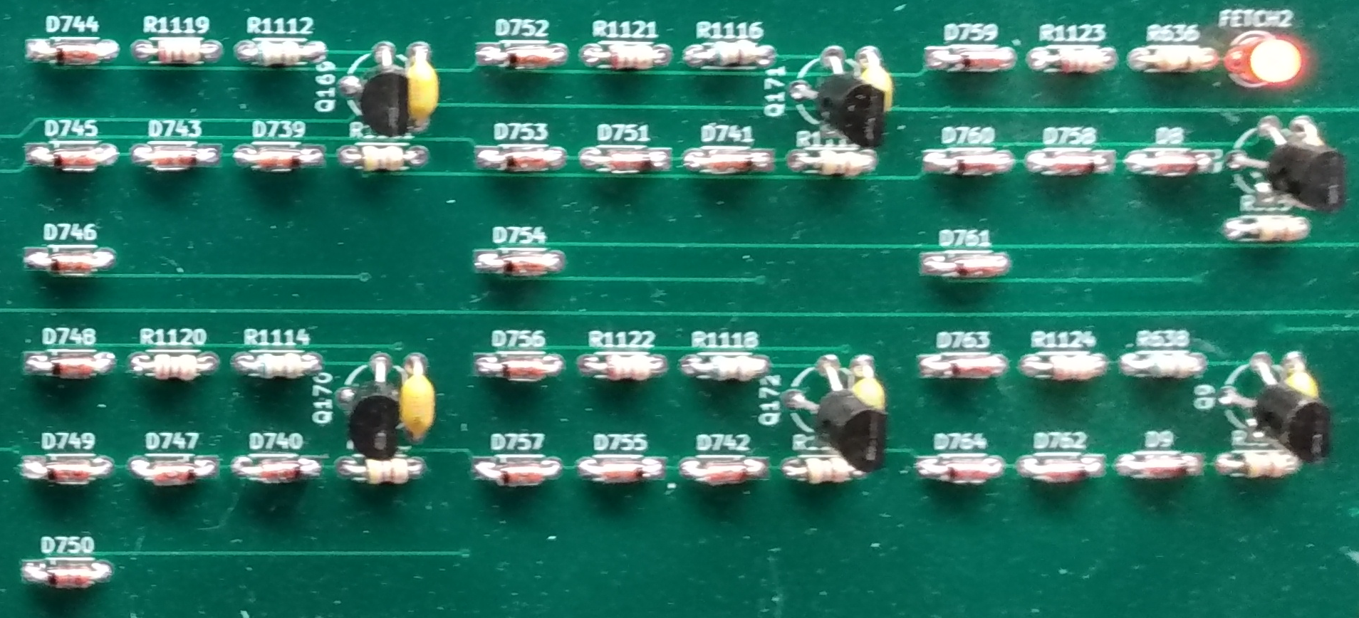
unit tests (one per board type) use paddles to operate boards
latches are 4 2-input nand gates
similar raspi level converters
* netgen
design written in simplified Verilog-like language
module, wire, assign
assign supports & | ~
built-in modules for connector, D-flipflop, latch, raspberry-pi
netgen java program compiles then simulates and generates
simulation scripts written in tcl (like qvartvs), simulates at gate level
generation creates kicad net and pcb files (looks like scheme) and a report
needs a map file for placement at gate and flipflop level
gate and flipflop internals are pre-routed
* raspictl
generates clock, reset, intreq signals
receives memread, memwrite, halt signals
operates bi-directional data bus
shadows processor state for verification
contains 64K byte array for memory
check for magic memory location (FFF0) access by processor for IO
used for synchronous syscalls
processor program generates an argument block somewhere in memory
...then writes its address to FFF0
RasPi then parses the argument block and performs corresponding IO
when IO is complete, RasPi resumes clocking the processor
processor program reads IO status from FFF0
currently does exit(), close(), gettimeofday(), open(), read(), write()
...also can assert/negate interrupt request line for testing
and simple println() call for debugging
can also generate random opcodes and operands for testing
* test programs
unit tests (one per board type) use paddles to operate boards
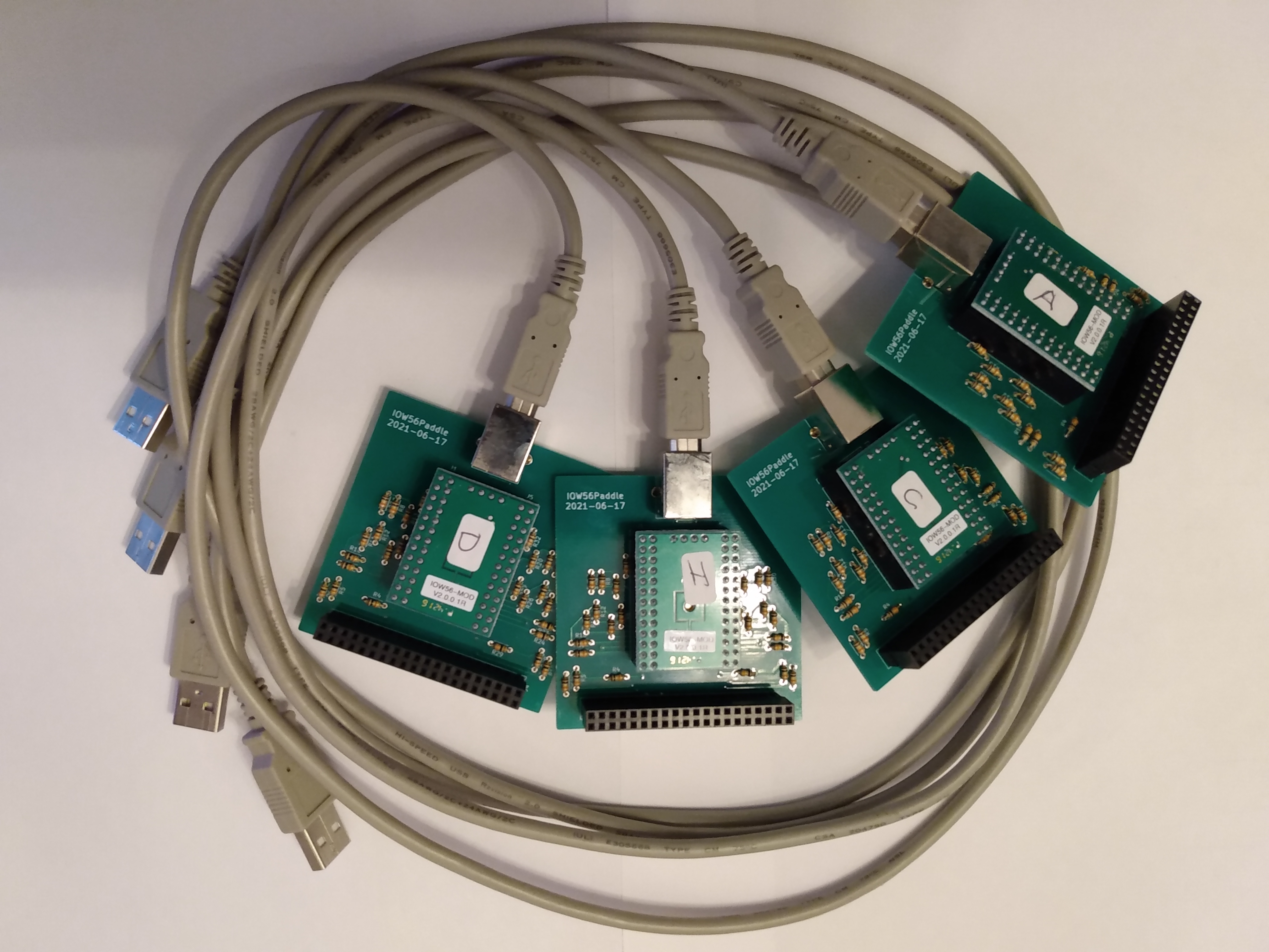 paddles are slow to write (200 Hz)
ras board needs gpio connected as well as paddles
running alutest on new alu board
paddles are slow to write (200 Hz)
ras board needs gpio connected as well as paddles
running alutest on new alu board
 integration test
generates random opcodes
minimum of seq, ras boards required
paddles required if no alu boards
any combo register boards
integration test
generates random opcodes
minimum of seq, ras boards required
paddles required if no alu boards
any combo register boards