There was no PDP-8/V made by Digital. So I am making one myself, Out Of Electron Valves.
The plan is there will be approx 320 tubes, specifically 6J6A. As of May 24, 2023, there is one board completed, the sequencer that contains the state flip-flops plus an instruction register latch (just the top four bits), and all the instruction decoding logic. That board uses 80 tubes, which is 160 gates. The tubes just do the inverting, the logic is done by crystal rectifiers. It runs at 28k cps.
Each tube has 2 triodes. A single triode is required to make an AND-OR-INVERT gate. Three tubes (6 triodes) are required to make a D flipflop (ahem, edge-triggered, bi-stable multivibrator). Two tubes (4 triodes) are needed to make a latch.
The tubes are just the processor. For memory and I/O, I use a Raspberry PI. Transistors are used to do the level conversion between the RasPI and the tubes and to drive the LEDs. At some point, I might change the front panel to neons or incandescents with tube drivers, but LEDs will do for now.
When all the boards are done, it will run slower than 28k cps as there will be more circuitry for the bits to work their way through (27 levels of logic for the full processor as opposed to 10 for just the sequencer board). So that implies the processor will come in somewhere around 10k cps, though I wouldn't be surprised at 5k cps cuz of longer circuit traces.
As of June 4, 2023, the memory address register board is complete, adding 48 tubes. The whole thing clocks at 25.5k cps.
There are going to be a total of five tubulated boards, the sequencer (completed), the MA register (completed), the PC register, the AC/Link register, and the ALU (next up). There are also the backplane board and transistorized front panel board as shown below.
More design details
Here is a video of just the sequencer and front panel running slowly (~5 cps) to see the lights blinking. The laptop is showing the RasPI output displaying the states. The FETCH-DEFER-EXEC-INTAK LEDs are stepping through the various states as the RasPI clocks the processor and sends it random opcodes. The top three bits of the instruction are shown in the IR LEDs. The RasPI checks the GPIO pins at the end of each cycle to make sure they are what they should be, as the RasPI knows what state the processor should be in for every cycle.
 |
sequencer board - 80 tubes - the crystal rectifiers are on the back |
 |
sequencer board crystal rectifiers (and fan pointed at the tubes!) |
 |
front panel - the whole thing is tipped on its side. RasPI is in bottom center of pic mounted to front panel board. |
 |
8-tube board - the 80 tubes on the sequencer board are really 10 of these boards, all identical, each containing 16 generic inverters.
They plug into the back of the large crystal rectifier board which gives them their individual personality.
32 more of these boards will have to be constructed, and plugged into the crystal rectifier boards,
to complete the PDP-8/V. Each 8-tube board requires +120V@45mA, -96V@35mA, +5V@10mA, 48V@400mA (8 6V filaments wired in series). The allocation of the 8-tube boards to the crystal rectifier boards are:
|
 |
the SEQ board with one of the 8-tube boards removed |
When all said and done, I estimate it will use about a kilowatt of power total, about the same amount as a small space heater.
Here is another video, this one shows the processor running at 28k cps. Again, the RasPI verifies the GPIO pins at the end of each cycle to make sure it is working correctly. If I speed it up to 30k cps, the RasPI is quick to catch the errors.
Early on, there were the:
You may also be interested in the Hode retro-computing project.
 |
8-tube board section each 8-tube board contains 16 of these KiCad project |
 |
Making an and-or-invert gate with crystal rectifiers and an 8-tube board section The internal wiring of the parts is contained in StandCell.java |
 |
D-flipflop from 6 NAND gates (diagram from Wikipedia)
The wiring of the A,B,C,D,E,F gates of the DFFs used in the PDP-8/V is contained in DFFModule.java , look for function setInputs() |
STATES
| FETCH1 | RasPI.Data,ALU = PC RasPI.MemRead = 1 | ⇨ FETCH2 |
| FETCH2 | IR ← RasPI.Data MA ← ALU = PC,RasPI.Data PC ← PC + 1 | ⇨ DEFER1 or EXEC1 |
| DEFER1 | RasPI.Data,ALU = MA RasPI.MemRead = 1 RasPI.MemWrite = auto-increment ? 1 : 0 | ⇨ DEFER2 |
| DEFER2 | MA ← RasPI.Data | ⇨ EXEC1 or DEFER3 |
| DEFER3 | MA ← RasPI.Data,ALU = MA plus 1 | ⇨ EXEC1 |
| EXEC1/AND | RasPI.Data,ALU = MA RasPI.MemRead = 1 RasPI.DFrame = IR[indir] | ⇨ EXEC2/AND |
| EXEC2/AND | AC ← ALU = AC and RasPI.Data | ⇨ FETCH1 or INTAK1 |
| EXEC1/TAD | RasPI.Data,ALU = MA RasPI.MemRead = 1 RasPI.DFrame = IR[indir] | ⇨ EXEC2/TAD |
| EXEC2/TAD | MA ← ALU = RasPI.Data | ⇨ EXEC3/TAD |
| EXEC3/TAD | Link,AC ← ALU = Link,AC plus MA | ⇨ FETCH1 or INTAK1 |
| EXEC1/ISZ | RasPI.Data,ALU = MA RasPI.MemRead = 1 RasPI.MemWrite = 1 RasPI.DFrame = IR[indir] | ⇨ EXEC2/ISZ |
| EXEC2/ISZ | MA ← ALU = RasPI.Data | ⇨ EXEC3/ISZ |
| EXEC3/ISZ | RasPI.Data,ALU = MA plus 1 PC ← PC + carry | ⇨ FETCH1 or INTAK1 |
| EXEC1/DCA | RasPI.Data,ALU = MA RasPI.MemWrite = 1 RasPI.DFrame = IR[indir] | ⇨ EXEC2/DCA |
| EXEC2/DCA | RasPI.Data,ALU = AC AC ← 0 | ⇨ FETCH1 or INTAK1 |
| EXEC1/JMS | RasPI.Data,ALU = MA RasPI.MemWrite = 1 RasPI.Jump = 1 | ⇨ EXEC1/JMS |
| EXEC2/JMS | RasPI.Data,ALU = PC | ⇨ EXEC2/JMS |
| EXEC3/JMS | PC ← RasPI.Data,ALU = MA plus 1 RasPI.MemRead = RasPI.IntReq ? 0 : 1 | ⇨ FETCH2 or INTAK1 |
| EXEC1/JMP | PC ← RasPI.Data,ALU = MA RasPI.MemRead = RasPI.IntReq ? 0 : 1 RasPI.Jump = 1 | ⇨ FETCH2 or INTAK1 |
| EXEC1/IOT | RasPI.Data,ALU = AC RasPI.Link = Link RasPI.IOInst = 1 | ⇨ EXEC2/IOT |
| EXEC2/IOT | AC ← ALU = RasPI.Data Link ← RasPI.Link PC ← PC + RasPI.IOSkip | ⇨ FETCH1 or INTAK1 |
| EXEC1/Group1 | AC ← ALU = AC modified by instruction | ⇨ FETCH1 or INTAK1 |
| EXEC1/Group2 | PC ← RasPI.Data,ALU = PC + skip ? 1 : 0 RasPI.MemRead = RasPI.IntReq ? 0 : 1 if CLA, AC ← 0 | ⇨ FETCH2 or INTAK1 |
| INTAK1 | RasPI.IntAck = 1 MA ← RasPI.Data,ALU = 0 RasPI.MemWrite = 1 IR ← JMS 0 | ⇨ EXEC2/JMS |
GPIO BUS - The GPIO Bus connects the processor to the Raspberry PI via the RasPI GPIO connector. Direction is from perspective of RasPI.
| CLOCK | Out | clock from RasPI, rising edge marks beginning of new cycle |
| DENA | Out | asserted: DATA/LINK is an input (tubes ⇨ RasPI) |
| IOS | Out | processor should skip next instruction (valid in EXEC2/IOT only) |
| IRQ | Out | RasPI is requesting an interrupt (synchronized with falling edge of clock) |
| QENA | Out | asserted: DATA/LINK is an output (RasPI ⇨ tubes) |
| RESET | Out | asynchronous reset from RasPI, asserted resets processor to FETCH1 state with PC = 0 |
| DATA | Bi | bi-directional 12-bit data bus |
| LINK | Bi | bi-directional link-bit bus (IO instructions only) |
| DFRM | In | the memory address given is in the current DATA frame |
| IAK | In | acknowledge interrupt (RasPI should negate interrupt request IRQ) |
| IOIN | In | IO instruction being executed (including Group 2 with HLT and/or OSR, and Group 3) (asserted during EXEC1 only) |
| JUMP | In | jump (JMP/JMS) instruction being executed (asserted during EXEC1 only) |
| READ | In | perform a memory read operation (memory address this cycle, data next cycle) |
| WRITE | In | perform a memory write operation (memory address this cycle, data next cycle) |
    Block diagram:

            ma  --------------------<-------------------------------------<-------+
            mq          ac  --------<-------------------------------------<---+   |
            pc          +1                                                    |   |
            -1          -1                                                    |   |
             0           0                                                    |   |
        +---------------------+                                               |   |
        |    A           B    |                                               |   |
        |         ALU         |                                               |   |
        |          Q          |                                               |   |
        +---------------------+                                               |   |
                   |                                                          |   |
                   +---------------->------ rotator -------   AC,LINK  --->---+   |
                   |                                                              |
                   +---------------->----------------------   MA       --->-------+
                   |                                                              |
                   +---------------->----------------------   PC       --->-------+
                   |                                                              |
                   +---------------->----------------------   RasPI    --->-------+--->---  IR/SEQ
ALU functions:
Backplane signals:
| • output by ACL (accumulator,link) board | |
| ACQ<11:00> | accumulator contents |
| ACQZERO | accumulator contents is zero |
| GRPB_SKIP | assuming doing group 2 arithmetic, it would skip |
| _LNQ,LNQ | link regiser contents |
| • output by ALU (arithmetic logic unit) board | |
| _ALUCOUT | carry output from ALU |
| _ALUQ<11:00> | ALU output |
| _NEWLINK | new link register contents |
| • output by MA (memory address register) board | |
| _MAQ<11:00>
MAQ<11:00> | MA register contents |
| • output by PC (program counter register) board | |
| PCQ<11:00> | PC register contents |
| • output by RPI (raspberry pi) board | |
| CLOK2 | clock |
| INTRQ | raspberry pi simulated IO device is requesting interrupt |
| IOSKP | the IO instruction wants to skip the next instruction |
| MQL | new link register contents from raspberry pi IO instruction |
| MQ<11:00> | raspberry pi memory location contents or accum value for IO instruction |
| RESET | reset the processor |
| • output by SEQ (sequencer) board | |
| _AC_ALUQ | load AC from ALU output at end of cycle |
| _AC_SC | load AC with zeroes at end of cycle |
| _ALU_ADD | ALU performs ALUA + ALUB |
| _ALU_AND | ALU performs ALUA & ALUB |
| _ALUA_M1 | select 7777 for ALU A operand |
| _ALUA_MA | select MA register for ALU A operand |
| ALUA_MQ0600 | select MQ<06:00> for ALU A<06:00> operand |
| ALUA_MQ1107 | select MQ<11:07> for ALU A<11:07> operand |
| ALUA_PC0600 | select PC<06:00> for ALU A<06:00> operand |
| ALUA_PC1107 | select PC<11:07> for ALU A<11:07> operand |
| ALUB_1 | select 0001 for ALU B operand |
| _ALUB_AC | select AC for ALU B operand |
| _ALUB_M1 | select 7777 for ALU B operand |
| _DFRM | memory operation being performed is in DFRAME |
| _GRPA1Q | in EXEC 1 state for group 1 arithmetic instruction |
| INC_AXB | ALU performs (A ^ B) + 1 |
| _INTAK | interrupt is being acknowledged |
| IOINST | performing an IO instruction |
| IOT2Q | in EXEC2 state for an IO instruction |
| IRQ<11:09> | top 3 bits of instruction register |
| _JUMP | doing a JUMP (JMP,JMS) instruction |
| _LN_WRT | write link register at end of cycle |
| _MA_ALUQ | load MA register from ALU output at end of cycle |
| _MREAD | perform memory read cycle |
| _MWRITE | perform memory write cycle |
| _PC_ALUQ | load PC register from ALU output at end of cycle |
| _PC_INC | increment PC register at end of cycle |
| TAD3Q | in EXEC3 state for a TAD instruction |
| FETCH{1,2}Q | in the given FETCH state (for front panel LEDs) |
| DEFER{1,2,3}Q | in the given DEFER state (for front panel LEDs) |
| EXEC{1,2,3}Q | in the given EXEC state (for front panel LEDs) |
| INTAK1Q | in the INTAK state (for front panel LEDs) |
Note:
More design details
Update as of May 28, 2023
 |
front panel standing up video standing up |
 |
+120V power supply with 80 tubes plugged in |
 |
other power supplies with 80 tubes plugged in the filament power supply is on the left with the big capacitor on a piggy-back circuit board to soft-start the filaments |
Update as of June 4, 2023
 |
sequencer and memory address boards total of 80 + 48 = 128 tubes! video of MA register countdown test program |
 |
power supplies with sequencer and memory address boards the -96V supply shows 96.06V 536mA 51.48W (from above pic) |
 |
running test program at 25+k cps short video |
Update as of June 7, 2023 - ALU board ordered
Update as of June 20, 2023 - Well, the whole thing ran with the ALU board for about 10 minutes (at 16k cps)!
Then things started going nuts, so the honeymoon is over!
I'm going to make some paddles for unit testing the boards, similar to the Hode paddles 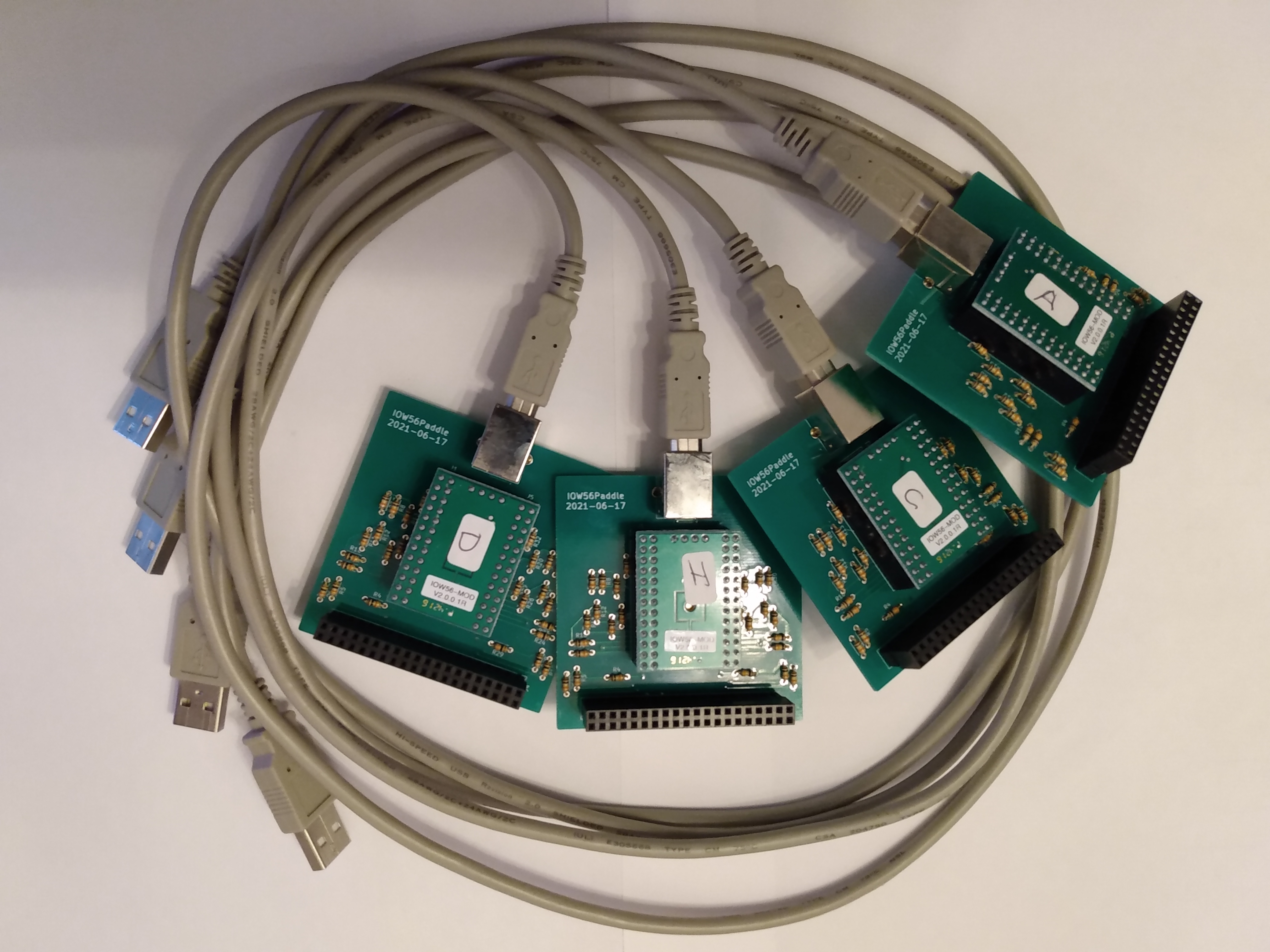 .
The chips can only handle -0.5V to +5.5V so the new paddles will need Schottkys for clamping. The big tube boards have 4 32-pin single-row
connectors so the new paddles will have to be designed for all that. They can plug into the USB ports of a RasPI or a Linux PC that will run test
programs to find problems.
.
The chips can only handle -0.5V to +5.5V so the new paddles will need Schottkys for clamping. The big tube boards have 4 32-pin single-row
connectors so the new paddles will have to be designed for all that. They can plug into the USB ports of a RasPI or a Linux PC that will run test
programs to find problems.
Anyway, the 16k cps is encouraging as there are only a couple more layers of logic around the longest path (27 vs 25). So theoretically, the final
processor should run somewhere near that, hoping for 10k or better at this point.
Update as of July 4, 2023 - Stupid paddles  , the IOWarriors have internal pullups and so load the tubes down too much.
So I have designed new paddles with 2N7000 buffers, hopefully they will work. That's about $200 down the twaletty.
, the IOWarriors have internal pullups and so load the tubes down too much.
So I have designed new paddles with 2N7000 buffers, hopefully they will work. That's about $200 down the twaletty.
Update as of July 18, 2023 - Got the new paddles working and testing the ALU board. The paddles are very slow but what the heck they run. I have some new IOWarrior-100 chips on order hopefully will speed it up.
 |  | |
| tube side of ALU board with new paddles | crystal rectifier side of ALU board with new paddles | |
| short video running test program | ||
The test program shown in the video simulates all the boards and provides inputs required to the ALU board via the paddles (highlighted in blue on the screen). At the end of each cycle, the test program reads all the outputs from the ALU board (highlighted in red) via the paddles and checks to make sure they are correct. It generates random instructions for the simulator to generate the test cases. I also have a test program that directly generates random numbers to feed to the ALU for testing. Both programs show the ALU is working.
There are a bunch of test clips you might notice on the tube side. Turns out a digitally keyed parts supplier sent me a bunch of 3.6V zener diodes when I had ordered 3.0V zeners. They were marked by the manufacturer as 3.0V (we looked at them under the microscope and they showed 3V0B), so it isn't the supplier's fault. Those clips go to a couple resistors to fudge the cathode bias down from 3.6V to 3.0V. At any rate, it seems to work equally well with 3.0V, 3.3V and 3.6V so I'm going to leave those zeners in unless they cause problems (the output voltages from the tubes would be a little higher with 3.6V for cathode bias instead of 3.0V). Measuring a heavily loaded point, the zero is well negative (-3V) coming out of the voltage divider with the cathode at 3.6V, so that's plenty good enough. I should do some more measurements (now that I have a couple hundred test cases) before building new boards to decide which zeners to use going forward.
Update as of August 20, 2023 - Have all constructed boards working with paddles, SEQ, MA, ALU, RPI.
GPIO is driven over WiFi so it occasionally pauses, and the fastest I can drive the paddles is around 30Hz. But that's good enough for testing at this point.The last video shows the test program. Red stuff is output from the boards onto the busses such as ALUQ, MAQ. Blue stuff is signals being generated by the paddles, such as AC, PC cuz I don't have the AC and PC boards yet. Also at the bottom in blue are signals being output by the GPIO pins such as CLOCK, IRQ (interrupt request). The DATA line alternates red and blue because it is bi-directional for the data being sent between the RasPI and the tubes.
I have physically re-arranged things because I bought an infrared camera. It showed some of the resistors on the tube boards were running at 180..190°F and the max they are rated for is 160°F (70°C). Now I have a fan basically for each board and now the resistors run around 120°F max. So I'm going to have to re-think the backplane to make room for more cooling for the last two boards (PC and AC/Link).
Update as of October 27, 2023
Video with RPI, SEQ, MA, ALU, ACL boards in place - total of 264 tubes so far.

Update as of October 28, 2023
Update as of November 12, 2023

All boards are put together and tested (at least for a couple hours). It clocks at 13+ kcps. It runs OS/8 using an emulated RK05.
 pic of some tube boards (SEQ on left, ALU, ACL on right)
 pic of some more tubes in back (backside of ACL on left with paddles, tubeside of PC on right)

Built a box to hold everything.
Later that afternoon: Plugged in the ACL (accumulator and link) board. Power use, including 2 fans, is 766 watts, power factor 0.96.

It seems happy running at 18 kcps with an asterisk. The cycles that involve an ADD are run slower than all the other cycles due to the many logic levels, even with carry look-ahead.
 |
 |
 | ||
| Front View | Right View (with fans removed) | Rear View | ||
|
|
|
That's pretty much it for the construction of the PDP-8/V! It runs at 18 kcps, uses 1.75 kW and weighs 130 lbs.
I have access to an ASR-33 but its printer doesn't work all that well. It likes to sometimes print C instead of A and misses processing CR about half the time so needs work.
Here's a video of it running the Conway's Life for the PDP-8. I added an Hobbs meter at the top right. It shows 2.3 or so, but the computer probably has been run around 10 hours total to date.
Playing with the high voltages, the processor runs with the negative voltage from -78V to -96.6V, and the positive from +110V to +128V. I previously thought it was very sensitive to voltage, but turns out it can be varied quite a bit. So then I set the voltages to mid-range, using -87.3V and +117.2V. The processor is now happy running at 25 kcps, a 38% improvement over the previous 18 kcps! And it's more eco-friendly, 1.71 kW, down from 1.75 kW. Hobbs 5.1.
The Zynq FPGA simulator would not run one of my tests, the one that tests the ACL (accumulator/link) board in isolation (autoboardtest -zynqlib -verbose acl). So digging into it with the Zynq's built-in logic analyzer, I saw that I was giving the LINK flipflop a very wimpy clock pulse, basically just a glitch. So I decided to fix the circuit to give it a full size clock pulse like (presumably) everything else. Fortunately it was a fairly simple patch that I could apply to the existing circuit board. But first, the circuit board had to be taken out of the box. So I tipped it over on its side (yes the box was designed to do that):

Now I was hoping that it would let me clock it faster, because the failures of running too fast have been that the LINK would get messed up. I had chalked it up to just the carry from doing a TAD not propagating fast enough, though sometimes it would fail from doing a rotate as well. Well at least I figured out why, it was the clocking that was messed up, not the carry as such. Anyway, it doesn't seem to be able to run much faster with the patch (couple 100 cps or so), but it was worth the work to track it down and fix it. Here it is chugging along at just over 25 kcps:
